Controlling the DP0POL switching matrix with daisy chained MAX4820: Unterschied zwischen den Versionen
Dl8rds (Diskussion | Beiträge) (→TEST) |
Dl8rds (Diskussion | Beiträge) (→TEST) |
||
| Zeile 344: | Zeile 344: | ||
Here is the ASCII table, together with the binary representations: | Here is the ASCII table, together with the binary representations: | ||
| − | [[Image:2018-10-27- | + | [[Image:2018-10-27-ascii_conversion_chart.gif]] |
As a test, I was using the input characters '*' and 'U', being nearly binary antagonists, while still being characters on my keyboard. | As a test, I was using the input characters '*' and 'U', being nearly binary antagonists, while still being characters on my keyboard. | ||
Version vom 27. Oktober 2018, 13:23 Uhr
Inhaltsverzeichnis
1 Background
DP0POL / DP0GVN is an amateur radio station on Neumayer3 station in Antarctica, hosting a unique WSPR station. As I have described in my article Red Pitaya Based WSPR Beacon for Antarctica DP0GVN, how the Red Pitaya platform of the first version was built, we now envisage another version 2:
It will be a 19" rack housing two (or possiby even four) Red Pitaya platforms. The reason is that the standard WSPR / FT8 software is only capale of processing EIGHT bands. However, we would want to monitor all shortwave bands, from long wave over the uneven bands up to 30 MHz.
Besides that, Antarctica is a rather tough place: The Antarctic winter brings us permanent darkness with temperatures possibly down to -50°C and since the antenna field is about two kilometers away from the main station, the SDR platforms will be literally out of reach for human beings. It is like a station on another planet. I guess, living conditions on planet Mars are more comfortable than in the Antarctic winter.
It will be simply impossible to diagnose antenna faults, and in case of a defective Red Pitaya we want to be able to simply switch one Red Pitaya from one antenna to another.
This all will be feasible through a switching matrix built by Helmut Berka DL2MAJ.
The matrix therefore employs a special chip: The MAX4820.
Maybe you have read my article about power switching with bistable latching relays: 8 Port Passive PoE Injector, Managed and Fused. This project is using a combination of I2C controlled PCF7485 16bit serial extensions to steer 8 relays. However, the drive power is too weak to control the relays directly. So we still require a darlington relay driver chip ULN2803 to drive the 5V relays there.
In the Antarctica project the number of relays is a little bigger: The switching matrix holds a total of 28 relays and thus leaves little space for I2C and driver chips. Besides that, I2c has the major disadvantage that each I2C chip normally only has three jumpers fur a selectable bus address space of 2³ and thus a total of 8 chips of the same type on the same bus. Even though it could be enough data lines with 16 bit * 8 ICs, the effort is still quite complex.
Helmut chose another approach: The MAX4820 can be daisy chained and thus requires some very different approach, but you can set many, many more relays with it. In fact, you're not really limited at all, except through a rather complex digital handling technique.
According to the datasheet, the MAX4820 is compatible with the Microwire and/or SPI protocol. I found this statement still rather tricky, because pure SPI does not support the RESET data line, but instead you must take care of a reset signal yourself.
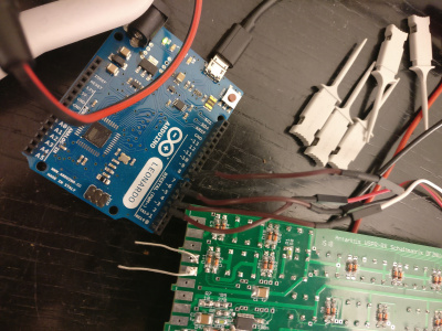
As a consequence, I decided against the implementation directly on a Raspberry Pi with my GPIOs, also given that the timing of the according signals was a little tricky. Instead, I chose an Arduino as the immediate controller platform, which now offers a USB standard interface and thus can be employed together with any arbitrary main computer.
This approach was also a response to the fact that there is no document on the web whatsoever, employing the keywords "MAX4820" together wirh "Raspberry" and "Python".
For this reason the Arduino drives my MAX4820 chain with all its control data lines and the Raspberry hosts the Python program that generates the integers over the serial connection that will again set the MAC ICs accordingly.
2 MAX4820
Here is the datasheet, first of all:
https://datasheets.maximintegrated.com/en/ds/MAX4820-MAX4821.pdf
Read it carefully!
The MAX4820 needs four main data lines:
- Serial Data (DIN). Sometimes also named "SDA".
- Serial Clock (SCL).
- Chip Select (CS): Drive CS low to select the device. When CS is low, data at DIN is clocked into the 8-bit shift register on SCLK’s rising edge. Drive CS from low to high to latch the data to the registers and activate the appropriate relays.
- Reset (RESET): Reset Input. Drive RESET low to clear all latches and registers (all outputs are turned off). RESET overrides all other inputs. If RESET and SET are pulledlow at the same time, then RESET takes precedence
The DOUT connects to the DIN of the next IC of the chain. Note that the prior chip eats up the first eight data bits and leaves nothing to its successor but what comes after those eight bits:
- Data Out (DOUT): Serial-Data Output. DOUT is the output of the 8-bit shift register. This output can be used to daisy chain multiple MAX4820s. The data at DOUT appears synchronous to SCLK’s falling edge.
Do not confuse the usage of SCL and SDA with I2C even though the naming is identical, this is no I2C at all. The MAX does not employ any addresses. There is really NO addressing whatsoever.
Here is how the interface is described in the datasheet:
The serial interface consists of an 8-bit shift register
and parallel latch controlled by SCLK and CS. The
input to the shift register is an 8-bit word. Each data bit
controls one of the eight outputs, with the most signifi-
cant bit (D7) corresponding to OUT8 and the least significant
bit (D0) corresponding to OUT1 (see Table 1).
When CS is low (device is selected), data at DIN  is
clocked into the shift register synchronously with SCLK’s rising
edge. Driving CS from low to high latches the data in the shift
register to the parallel latch.
DOUT is the output of the shift register. Data appears
on DOUT synchronously with SCLK’s falling edge and
is identical to the data at DIN delayed by eight clock
cycles. When shifting the input data, D7 is the first bit in
and out of the shift register. While CS is low, the switches always
remain in their previous state. Drive CS high after 8 bits of
data have been shifted in to update the output state and
inhibit further data from entering the shift register. When
CS is  high, transitions at DIN and SCLK have no effect
on the output, and the first input bit (D7) is present at DOUT.
If the number of data bits entered while CS is low is
greater or less than 8, the shift register contains only
the last 8 data bits, regardless of when they were
entered.
Here is how I implemented the interface:
- The standard period is 50 microseconds. Every time span will be a multiple of 50 microseconds.
- It makes sense to start with the RESET line going LO in order to set all the latches to ZERO disregarding their previous state. The RESET line can go back to HI after 5 times the standard timespan.
- Then we will start with Chip Select. We pull it to LO in order to enable programming. CS stays LO as long as there is programing activity on the DIN line.
- Then we start a loop:
- We write the due data bit, HI or LO as requested.
- After writing, we produce a rising flank and a falling flank. Since the data bit will be shifted into the according register with the rising flank, we must ensure to have the data bit set slightly before the clock comes around.
- After the end of the bits, there are no more clock cycles either.
- We rise CS to HI in order to activate the latching. This is the moment when the relays will be switched.
- Then we spend a long time of 50 Milliseconds in order to grant sufficient time to the relays to get the switching done.
- Finally we do another round of RESET for 5*standard timespans to make sure every bit is cleared again.
This will leave our relays in the situation that the coils still operate under power. Remember that we want to switch RF signals, so operating an inductive element in immediate proximity of a RF signal line is no good idea at all, we will need to remove power from all the coils.
The procedure is exactly the same as above, yet without any data bits. The Data In line can be left to LO and the rest of the procedure is carried out just alike.
Given that OUT1 and OUT2 are antagonists, as OUT3/OUT4, OUT5/OUT6 and OUT7/OUT8, it should be forbidden to set them at the same time. I will not implement any safety procedures in the Arduino code, because I think that the control interface should so clever as to do that at the other side. I follow the idea to keep the static part of the implementation as minimal as possible in order to allow as few incorrectible faults as possible.
3 Measurement
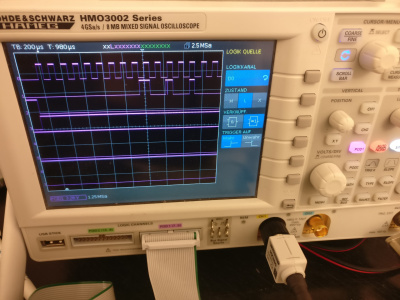
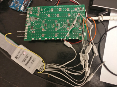
I am proud owner of a R&S HAMEG HMO-3024 mixed signals oscilloscope.
This device is capable of storing a vast number of samples, across all digital channels.
I was using the logic analysis part together with the manual trigger subsystem, where the trigger voltage was set to 3,3V and the logic trigger on the according channels that would start ahead, notably the RESET signal going LO.
4 Arduino Code
Here is my implementation:
#define DEBUG 0

#define MAX_CS 6        // /CS
#define MAX_SDA 3       // SDA
#define MAX_RESET 8     // /RESET
#define MAX_SCLK 4      // SCLK

#define IN_MAX 50       // maximale Einleselaenge PLUS CR oder LF

int Wartezeit = 50;     // Verzoegerung bei Datenausgabe, hier 50µs

byte i = 0;             // Laufvariable
byte j = 0;             // Laufvariable
byte x;                 // Laufvariable
int inByte = 0;         // incoming serial byte
int inDaten[IN_MAX];    // Eingehende Daten
bool inBool[IN_MAX*8];  // Eingehende Daten
int datenCounter = 0;   // Datenzaehler
const int max_len = IN_MAX;

void setup() {
  pinMode(MAX_RESET, OUTPUT);
  pinMode(MAX_CS, OUTPUT);
  pinMode(MAX_SDA, OUTPUT);
  pinMode(MAX_SCLK, OUTPUT);

  digitalWrite(MAX_RESET, LOW);   // alle Ausgaenge zuruecksetzen
  delayMicroseconds (Wartezeit);
  digitalWrite(MAX_CS, HIGH);     // keinen Baustein selektieren
  delayMicroseconds (Wartezeit);
  digitalWrite(MAX_SDA, LOW);     // SDA=Din bei MAX4820 auf low setzen
  delayMicroseconds (Wartezeit);;
  digitalWrite(MAX_SCLK, LOW);    // SCLK bei MAX4820 auf low setzen
  delayMicroseconds (Wartezeit);
  digitalWrite(MAX_RESET, HIGH);  // Bausteine freigeben fuer Programmierung
  delayMicroseconds (Wartezeit);

  // start serial port at 9600 bps:
  Serial.begin(9600);
  while (!Serial) {
    ; // wait for serial port to connect. Needed for native USB port only
  }
  delay(100); // 100ms warten
  Serial.print("OK >> ");

}

void SignalAusgabe(bool inBool[IN_MAX * 8], int datenCounter) {

  Serial.print("Signalausgabe, Zeichen ohne CR|LF >");
  Serial.println(datenCounter - 1);

  // /RESET setzen
  /*
  RESET: Reset Input. Drive RESET low to clear all latches and registers
  (all outputs are turned off). RESET overrides all other inputs. If
  RESET and SET are pulled low at the same time, then RESET takes
  precedence.
  */
  digitalWrite(MAX_RESET, LOW); // alle Ausgaenge deaktivieren (open Drain, Impulsrelais !!! )
  delayMicroseconds(5* Wartezeit);
  digitalWrite(MAX_RESET, HIGH);  // Bausteine freigeben fuer Programmierung

  // /CS aktivieren
  /*
  CS: Drive CS low to select the device. When CS is low, data at DIN is
  clocked into the 8-bit shift register on SCLK’s rising edge. Drive CS
  from low to high to latch the data to the registers and activate the
  appropriate relays.
  */
  digitalWrite(MAX_CS, LOW);
  delayMicroseconds (Wartezeit);

  for (int l = 0; l < (datenCounter -1 ) * 8; l++) {

    if (inBool[l] == 1) {
      digitalWrite(MAX_SDA, HIGH);

    } else {
      digitalWrite(MAX_SDA, LOW);

    }

    // Takterzeugung
    digitalWrite(MAX_SCLK, HIGH); // Taktimpuls wird erzeugt, Daten werden uebernommen
    delayMicroseconds(Wartezeit);


    digitalWrite(MAX_SCLK, LOW); // Taktimpuls wird zurueckgenommen
    delayMicroseconds(Wartezeit);

  }
  digitalWrite(MAX_SDA, LOW);

  // /CS deaktivieren = Daten auf Ausgaenge schalten
  digitalWrite(MAX_CS, HIGH);

#if DEBUG==1
  delayMicroseconds(10* Wartezeit);  // schnell, fuers Oszilloskop
#else
  delay(50); // 50ms warten
#endif

  // Sicherheitshalber danach auch noch mal RESET setzen
  /*
  RESET: Reset Input. Drive RESET low to clear all latches and registers
  (all outputs are turned off). RESET overrides all other inputs. If
  RESET and SET are pulled low at the same time, then RESET takes
  precedence.
  */
  digitalWrite(MAX_RESET, LOW); // alle Ausgaenge deaktivieren (open Drain, Impulsrelais !!! )
  delayMicroseconds(5* Wartezeit);  // nur alternativ zum Debugging
  digitalWrite(MAX_RESET, HIGH);  // Bausteine freigeben fuer Programmierung

  // Und jetzt kommt die Zurücksetzung der ganzen Relais

    // /CS aktivieren
  /*
  CS: Drive CS low to select the device. When CS is low, data at DIN is
  clocked into the 8-bit shift register on SCLK’s rising edge. Drive CS
  from low to high to latch the data to the registers and activate the
  appropriate relays.
  */
  digitalWrite(MAX_CS, LOW);
  delayMicroseconds (Wartezeit);

  // Wir wollen alle Kanaele auf NULL Schalten
  digitalWrite(MAX_SDA, LOW);

  for (int l = 0; l < (datenCounter -1 ) * 8; l++) {

    // Takterzeugung
    digitalWrite(MAX_SCLK, HIGH); // Taktimpuls wird erzeugt, Daten werden uebernommen
    delayMicroseconds(Wartezeit);


    digitalWrite(MAX_SCLK, LOW); // Taktimpuls wird zurueckgenommen
    delayMicroseconds(Wartezeit);

  }
  digitalWrite(MAX_SDA, LOW);

  // /CS deaktivieren = Daten auf Ausgaenge schalten
  digitalWrite(MAX_CS, HIGH);

#if DEBUG==1
  delayMicroseconds(10* Wartezeit);  // schnell, fuers Oszilloskop
#else
  delay(50); // 50ms warten
#endif

  // Sicherheitshalber danach auch noch mal RESET setzen
  /*
  RESET: Reset Input. Drive RESET low to clear all latches and registers
  (all outputs are turned off). RESET overrides all other inputs. If
  RESET and SET are pulled low at the same time, then RESET takes
  precedence.
  */
  digitalWrite(MAX_RESET, LOW); // alle Ausgaenge deaktivieren (open Drain, Impulsrelais !!! )
  delayMicroseconds(5* Wartezeit);  // nur alternativ zum Debugging
  digitalWrite(MAX_RESET, HIGH);  // Bausteine freigeben fuer Programmierung

}


void loop() {
  // if we get a valid byte, read analog ins:
  if (Serial.available() > 0) {
    // get incoming byte:
    inByte = Serial.read();

    Serial.print("datenCounter >");
    Serial.println(datenCounter);

    if (datenCounter < max_len) {
      Serial.print("Zeichen akzeptiert BIN>");
      Serial.print(inByte, BIN);
      Serial.print("< DEC>");
      Serial.print(inByte, DEC);
      char o = inByte;
      Serial.print("< CHA>");
      Serial.println(o);
      inDaten[datenCounter] = inByte;
      datenCounter++;
    } else {
      Serial.println("datenCounter OVERRUN");
      datenCounter = 0;
      for (int i = 0; i < max_len; i++) {
        inDaten[i] = 0;
      }
    }

    if ((inByte == 10) || (inByte == 13)) {
      // Abarbeitung
      for (int n = 0; n < datenCounter; n++) {
        for (int i = 0; i <= 7; i++) {
          inBool[n * 8 + i] = bitRead(inDaten[n], i);
        }
      }

      Serial.print("OUT>>>>>");
      for (int n = 0; n < datenCounter - 1; n++) {
        for (int i = 0; i <= 7; i++) {
          Serial.print(bitRead(inDaten[n], i));
        }
        if (n < datenCounter - 2)
          Serial.print(".");
      }
      Serial.print("<<<<<OUT");
      Serial.println();

      SignalAusgabe(inBool, datenCounter);

      // nach Verarbeitung setze alles auf NULL
      datenCounter = 0;
      for (int i = 0; i < IN_MAX; i++) {
        inDaten[i] = 0;
        for (int n = 0; n <= 7; n++) {
          inBool[i * 8 + n] = 0;
        }
      }

      Serial.print("OK >> ");

    }

  }
}
5 TEST
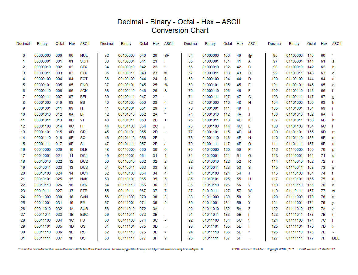
Here is the ASCII table, together with the binary representations:
As a test, I was using the input characters '*' and 'U', being nearly binary antagonists, while still being characters on my keyboard.
Here is the dialog of the serial monitor:
5.1 First Test
datenCounter >0
Zeichen akzeptiert BIN>101010< DEC>42< CHA>*
datenCounter >1
Zeichen akzeptiert BIN>101010< DEC>42< CHA>*
datenCounter >2
Zeichen akzeptiert BIN>1101< DEC>13< CHA>
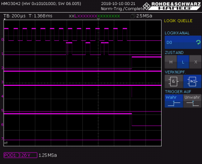
OUT>>>>>01010100.01010100<<<<<OUT
Signalausgabe, Zeichen ohne CR|LF >2
resulting in the following logic diagram:
5.2 Second Test
datenCounter >0
Zeichen akzeptiert BIN>1010101< DEC>85< CHA>U
datenCounter >1
Zeichen akzeptiert BIN>1010101< DEC>85< CHA>U
datenCounter >2
Zeichen akzeptiert BIN>1101< DEC>13< CHA>
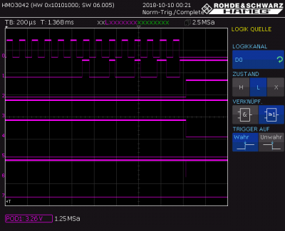
OUT>>>>>10101010.10101010<<<<<OUT
Signalausgabe, Zeichen ohne CR|LF >2
resulting in the following logic diagram:
6 Python Code
Will be posted here later!!!
